




 BOM
 Cart
 Product Catalog
The ADS1256 is a high-precision 24-bit analog-to-digital converter (ADC) developed by Texas Instruments for applications that require accurate, low-noise signal measurement. It combines a delta-sigma (ΔΣ) converter, a programmable gain amplifier (PGA), a flexible input multiplexer, and a programmable digital filter to provide reliable measurements from a variety of analog sensors.
With eight single-ended input channels or four differential input channels, the chip is suitable for data acquisition systems, industrial process control, scientific instruments, electronic weighing scales, and test equipment. It supports SPI-compatible communication, data rates up to 30,000 samples per second (SPS), and programmable gain settings from 1 to 64.
This guide covers the ADS1256 chip description, pinout, specifications, key features, applications, Arduino UNO wiring, and the main characteristics of an ADS 1256 24-bit 8-channel ADC module.
1. Description of the ADS1256 Chip
7. ADS1256 24-bit 8-channel ADC Module
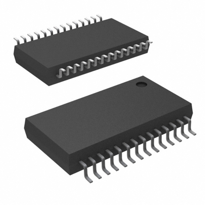
Description of the ADS1256 Chip
The ADS1256 is a high-resolution, low-noise ADC designed to convert small analog signals into digital data with high precision. It is part of the ADS1255/ADS1256 family from Texas Instruments, which provides complete measurement solutions for demanding applications where signal accuracy and stability are important.
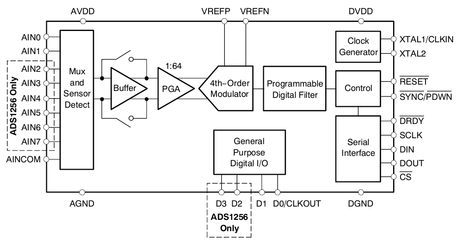
The device uses a fourth-order delta-sigma modulator followed by a programmable digital filter. This architecture helps reduce noise and achieve high measurement resolution. Under suitable operating conditions, the converter can provide up to 23 bits of noise-free resolution, with data output rates reaching 30 kSPS.
One of its main advantages is the integrated programmable gain amplifier. The PGA offers gain settings from 1 to 64 in binary steps, allowing low-level sensor signals to be amplified before conversion. A selectable input buffer can also increase input impedance, helping reduce the loading effect on external sensors.
The ADS 1256 includes a flexible input multiplexer that supports eight single-ended inputs or four differential inputs. This makes it possible to measure multiple sensors with a single ADC rather than requiring a separate converter for each signal. The multiplexer also includes sensor-detection functionality to help verify the integrity of connected sensors.
For communication, the device uses an SPI-compatible serial interface with a 5 V-tolerant digital interface, while its digital supply operates from 1.8 V to 3.6 V. Additional functions include self-calibration, system calibration, fast channel cycling, single-cycle settling for one-shot conversions, four general-purpose digital I/O pins, and a programmable clock output.
The ADS1256 is available in a 28-pin SSOP package. The ADS1256 is particularly useful when a project needs high-resolution measurements from multiple analog inputs without significantly increasing circuit complexity.
ADS1256 Pinout
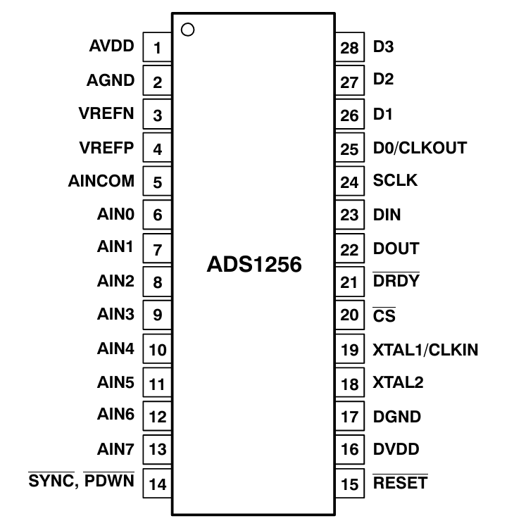
The ADS 1256 uses a 28-pin SSOP package. Its pins are divided into analog inputs, power connections, reference inputs, digital communication signals, clock connections, and general-purpose I/O.
Pinout and pin functions for the ADS1256 28-pin package.
Pin No. | Pin Name | Type | Description |
1 | AVDD | Analog power | Analog power supply |
2 | AGND | Analog ground | Analog ground connection |
3 | VREFN | Analog input | Negative reference input |
4 | VREFP | Analog input | Positive reference input |
5 | AINCOM | Analog input | Common analog input |
6 | AIN0 | Analog input | Analog input channel 0 |
7 | AIN1 | Analog input | Analog input channel 1 |
8 | AIN2 | Analog input | Analog input channel 2 |
9 | AIN3 | Analog input | Analog input channel 3 |
10 | AIN4 | Analog input | Analog input channel 4 |
11 | AIN5 | Analog input | Analog input channel 5 |
12 | AIN6 | Analog input | Analog input channel 6 |
13 | AIN7 | Analog input | Analog input channel 7 |
14 | SYNC/ PDWN | Digital input | Synchronization and power-down control |
15 | RESET | Digital input | Active-low reset |
16 | DVDD | Digital power | Digital power supply |
17 | DGND | Digital ground | Digital ground connection |
18 | XTAL2 | Digital | Crystal oscillator connection |
19 | XTAL1/ CLKIN | Digital input | Crystal connection or external clock input |
20 | CS | Digital input | Active-low chip select |
21 | DRDY | Digital output | Active-low data-ready signal |
22 | DOUT | Digital output | Serial data output |
23 | DIN | Digital input | Serial data input |
24 | SCLK | Digital input | SPI serial clock |
25 | D0/ CLKOUT | Digital I/O | Digital I/O 0 or clock output |
26 | D1 | Digital I/O | Digital I/O 1 |
27 | D2 | Digital I/O | Digital I/O 2 |
28 | D3 | Digital I/O | Digital I/O 3 |
Important ADS1256 Pin Functions
Analog inputs (AIN0–AIN7): These eight channels accept external analog signals. They can configure for single-ended or differential measurements through the input multiplexer. In single-ended operation, AINCOM can serve as the common input.
Reference inputs (VREFP and VREFN): These pins connect to the external voltage reference that determines the ADC's measurement scale. A stable, low-noise reference is important for achieving high measurement accuracy.
SPI communication pins: DIN, DOUT, SCLK, and CS handle serial communication with a microcontroller. DRDY indicates when ready to read conversion data.
Power pins: AVDD and AGND supply the analog section, while DVDD and DGND serve the digital section. Proper grounding, decoupling, and PCB layout help minimize interference between analog and digital signals.
Clock and control pins: XTAL1/CLKIN and XTAL2 provide clock connections. RESET restarts the device, while SYNC/PDWN supports synchronization and power-down control.
The digital inputs have Schmitt-trigger characteristics and are 5 V tolerant where specified. When using an external clock on XTAL1/CLKIN, XTAL2 should be left disconnected as directed by the device documentation.
Block Diagram
ADS1256 Specifications
The ADS 1256 combines a 24-bit delta-sigma ADC with a programmable gain amplifier and a multiplexed input architecture. Its specifications make it suitable for precision data acquisition systems that need to measure low-level signals across multiple channels.
Parameter | Value |
Manufacturer | Texas Instruments |
Resolution | 24 bits |
Maximum data rate | 30 kSPS |
Number of ADCs | 1 |
Number of input channels | 8 single-ended or 4 differential |
Input type | Differential, single-ended |
Architecture | Delta-sigma |
Configuration | MUX-PGA-ADC |
PGA gain | 1, 2, 4, 8, 16, 32, 64 |
Data interface | SPI-compatible |
Reference type | External |
Analog supply | 5 V nominal |
Digital supply | 1.8 V to 3.6 V |
Noise-free resolution | Up to 23 bits |
Maximum nonlinearity | ±0.0010% |
Normal-mode power dissipation | As low as 38 mW |
Standby power dissipation | Approximately 0.4 mW |
Operating temperature | -40°C to +85°C |
Package | 28-SSOP |
Mounting type | Surface mount |
The actual measurement performance depends on the selected data rate, PGA gain, reference voltage, input signal, and circuit layout. Although the output is 24 bits wide, not all 24 bits are necessarily noise-free under every operating condition.
ADS1256 Features
The converter provides several functions designed to improve measurement accuracy, simplify sensor interfacing, and reduce the need for additional external components.
High-Resolution 24-Bit Conversion
The 24-bit output provides a wide digital representation of the input signal, making the device suitable for applications involving small voltage changes. Its delta-sigma architecture and digital filtering help suppress unwanted noise, although the effective resolution depends on the measurement conditions.
Programmable Gain Amplifier
The integrated PGA supports gain settings from 1 to 64. Low-level signals from load cells, bridge sensors, and other analog transducers can therefore be amplified before conversion. Selecting an appropriate gain helps use the ADC's input range effectively without exceeding its permissible input limits.
Multiplexed Multi-Channel Measurements
The input multiplexer allows one converter to measure several signals. The eight analog inputs can configure for eight single-ended measurements or four differential measurements, making the device useful for multi-sensor data acquisition.
Calibration and Digital Filtering
Self-calibration and system calibration help correct offset and gain errors. The programmable digital filter allows designers to choose an appropriate balance between output rate and noise performance. These functions are particularly valuable in precision measurement systems where repeatability matters.
ADS1256 Applications
The ADS 1256 is suitable for applications that require high-resolution conversion, low-noise measurements, and flexible analog input configuration.
Scientific instrumentation: Laboratory instruments can use the converter to measure small voltage variations from experimental sensors. Its programmable gain and digital filtering help capture low-level signals for analysis and recording.
Industrial process control: The device can collect analog measurements from pressure sensors, temperature measurement circuits, and other industrial transducers. Multiple input channels allow a single converter to monitor several signals in a compact data acquisition system.
Medical equipment: Measurement instruments that acquire low-level analog signals can benefit from its resolution and low-noise architecture. The ADC is only one component of such systems; appropriate analog front-end design, isolation, calibration, and applicable medical safety requirements remain necessary.
Test and measurement equipment: Precision multimeters, data loggers, and electronic test systems can use the chip to convert analog signals into digital values for processing by a microcontroller or computer.
Electronic weighing scales: Load cells typically generate small differential voltage signals. The integrated PGA and differential inputs make the converter suitable for weighing systems that need higher resolution than many general-purpose microcontroller ADCs provide.
Multi-channel sensor monitoring: The eight-channel input multiplexer is useful for applications that need to monitor several analog sensors with a shared ADC, reducing the need for multiple independent conversion circuits.
Connecting ADS1256 to Arduino UNO
The ADS 1256 can communicate with an Arduino UNO through its SPI interface. The Arduino sends configuration commands to the ADC and reads the converted data through the serial interface. The DRDY pin indicates when new conversion data is available.
ADS1256 Arduino Wiring
ADS1256 Module | Arduino UNO |
5V | 5V |
GND | GND |
SCLK | Pin 13 (SCK) |
DIN | Pin 11 (MOSI) |
DOUT | Pin 12 (MISO) |
DRDY | Pin 9 |
CS | Pin 10 |
Wiring note: This table assumes a module designed to accept a 5 V supply. Check the module's specifications before connecting power. The bare ADS1256 chip uses a nominal 5 V analog supply and a 1.8 V to 3.6 V digital supply, so the chip itself should not be powered directly from the Arduino's 5 V logic rail on DVDD.
How to Use ADS1256 with Arduino
Step 1: Connect the hardware. Wire the SPI pins, chip-select pin, data-ready pin, power, and ground according to the table. Connect the analog signal to the appropriate input channel and ensure that the input voltage stays within the permitted operating range.
Step 2: Configure SPI communication. Initialize the Arduino SPI peripheral and configure the communication settings required by the ADC. The software must send the appropriate register-write and command sequences to initialize the device.
Step 3: Set the ADC parameters. Configure the input multiplexer, PGA gain, data rate, and digital filter. Select the reference voltage and input configuration according to the sensor being measured.
Step 4: Read the conversion data. Monitor DRDY to determine when the ADC has new data. Once the data is ready, read the conversion result through SPI and process the received bytes as a signed 24-bit measurement.
Step 5: Convert the result into a voltage. Use the ADC's configured reference voltage, PGA gain, and the correct signed-data conversion to calculate the input voltage. For differential measurements, the result represents the voltage difference between the selected positive and negative inputs.
Important Considerations
The ADS1256 is more complex to initialize than the built-in ADC on an Arduino UNO. A suitable driver library can simplify register configuration, channel selection, and data acquisition.
For accurate results, use a stable voltage reference, suitable input filtering, and careful grounding. The reference voltage and PGA gain must be included when converting the raw digital output into engineering units such as volts, temperature, pressure, or weight.
ADS1256 24-Bit 8-Channel ADC Module
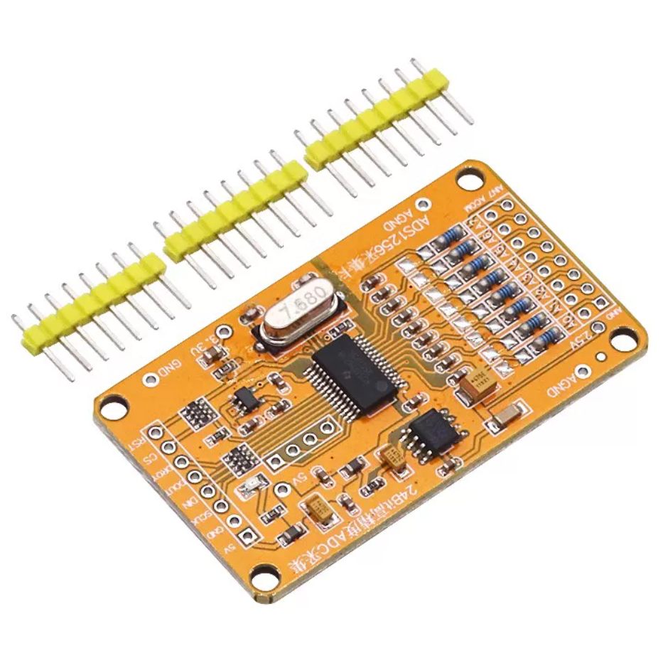
The ADS 1256 24-bit 8-channel ADC module is a development board built around the ADS1256IDBR converter. It integrates the ADC with a voltage-reference circuit, power regulation, input filtering, and other supporting components to simplify precision analog measurement.
Compared with using the bare chip, the module reduces the amount of external circuitry that developers need to design and assemble. It is useful for Arduino, STM32, Raspberry Pi, and other compatible systems when the correct voltage levels and communication interface are provided.
Main Module Features
Feature | Description |
ADC chip | ADS1256IDBR |
Resolution | 24 bits |
Analog input channels | A0–A7, eight channels |
Input configuration | Single-ended or differential |
Voltage reference | ADR03 2.5 V reference |
Reference buffering | OPA350 high-speed buffer |
Input filtering | Individual 104-marked capacitors, typically 100 nF |
Power regulation | Low-noise LDO with high power-supply rejection |
Power filtering | 100 µF tantalum capacitor and an inductor forming an LC filter |
Noise reduction | Low-noise metal-film resistors and high-frequency attenuation resistors |
PCB layout | Separate analog and digital ground routing |
Test points | GND, 2.5 V, and 3.3 V |
Low-Noise Voltage Reference
The module uses an ADR03 2.5 V reference with an OPA350 buffer. The reference circuit includes low-pass filtering intended to reduce noise, including low-frequency disturbances. Since the reference voltage directly affects conversion accuracy, this circuit is an important part of the module's measurement performance.
Input Filtering and Power Management
Each analog input has a filter capacitor to help attenuate unwanted high-frequency components. The low-noise LDO and LC power filter reduce supply disturbances that might otherwise affect the analog measurement circuitry.
Low-noise, low-temperature-coefficient metal-film resistors help improve stability, while additional resistors on digital signal lines can reduce high-frequency interference.
Analog and Digital Ground Separation
The board uses separate analog and digital ground routing to help reduce coupling from digital switching activity into sensitive analog signals. This layout approach is particularly important when measuring small voltages with a high-resolution ADC.
The additional GND, 2.5 V, and 3.3 V test points make it easier to check the power supply and reference circuit during troubleshooting.
What Should You Check Before Using the Module?
Before connecting the board to a microcontroller, verify its supply requirements, digital logic levels, pin assignments, reference voltage, and analog input range. Also confirm whether the particular module exposes all eight input channels and how it handles differential connections.
A 24-bit output does not automatically guarantee 24 noise-free bits. Actual performance depends on the sensor, reference circuit, PCB layout, input filtering, PGA setting, and selected data rate.
Frequently Asked Questions
What is ADS1256 price?
The price of an ADS1256 depends on whether you purchase the bare integrated circuit or a complete 24-bit, 8-channel ADC module. Module prices also vary according to PCB design, voltage-reference circuitry, component quality, and supplier. Check current distributor or electronics retailer listings to compare prices, stock availability, and shipping costs.
How to use ADS1256?
To use the ADS1256, connect a suitable power supply, a stable external voltage reference, the analog input signal, and an SPI-compatible microcontroller. Initialize the ADC, configure its input multiplexer, PGA gain, and data rate, then wait for DRDY to indicate that data is ready. Read the 24-bit result and convert it using the selected reference voltage and gain.
Is the ADS1256 Really a 24-Bit ADC?
Yes. The ADS1256 produces a 24-bit digital conversion result and is specified for no missing codes under its stated operating conditions. However, the effective resolution and noise-free resolution are lower in many practical configurations. The actual usable resolution depends on data rate, gain, input signal, reference quality, and circuit design.
Can the ADS1256 Measure Multiple Sensors?
Yes. Its integrated multiplexer supports eight single-ended input channels or four differential input channels. This allows a single ADC to measure multiple sensors sequentially. When switching channels, configure the multiplexer correctly and allow for the appropriate settling and conversion time before relying on the new measurement.
What Is the Difference Between ADS1255 and ADS1256?
Both devices are low-noise, 24-bit delta-sigma ADCs with programmable gain and SPI-compatible communication. The main difference is the input configuration and package. The ADS1256 supports eight single-ended or four differential inputs and uses a 28-pin SSOP package. The ADS1255 has fewer input channels and is supplied in a 20-pin SSOP package.
Conclusion
The ADS1256 is a versatile 24-bit ADC for applications that require high-resolution analog measurements, low-noise performance, and multi-channel input capability. Its programmable gain amplifier, flexible input multiplexer, digital filtering, calibration functions, and SPI interface make it suitable for scientific instrumentation, industrial monitoring, weighing systems, and precision data acquisition.
For developers, an ADS1256 8-channel ADC module provides a convenient starting point by integrating the chip with supporting power, reference, and filtering circuits. When paired with an Arduino UNO or another compatible microcontroller, it offers a practical way to build a high-resolution measurement system. Correct power connections, reference selection, input configuration, grounding, and data processing are essential for achieving reliable results.
Read More:
1. ADS1220 24-Bit ADC: Pinout, Alternatives, and Module Board
2. TP4057 Chip Single Lithium-Ion Battery Charger Guide
3. LM1117 Voltage Regulator: Pinout, Equivalent & Datasheet
ADS1256 Datasheet:
HOT NEWS
TP4056 Charging Module Pinout, Working, and Applications
TP4056 Charging Module Pinout, Working, and Applications
2026-01-23
LR41 Battery Guide: Specifications, Equivalents, and Uses
LR41 Battery Specifications, Equivalents, and Uses
2025-12-14
Understanding The CD4051 Analog Multiplexer
CD4051 analog multiplexer
2025-06-30
Understanding A 0603 Resistor
0603 resistor,dimensions,marking code, values
2025-05-29
MT3608 Boost Converter - An In-Depth Guide
MT3608 Boost Converter
2025-09-04
The 0402 Resistor: A Comprehensive Guide
0402 Resistor
2025-05-06
Complete Guide to the 220 Ohm Resistor
220 Ohm Resistor
2025-07-28
Mini MP1584 DC-DC 3A Buck Converter Module: Complete Guide
Mini MP1584 DC-DC 3A Buck Converter Module: Complete Guide
2026-03-26
Guide To The XL6009 Boost Converter
XL6009 Boost Converter
2025-09-05
What Is A 1206 Resistor?
1206 resistor dimensions,footprint,value
2025-06-05