


 BOM
BOM Cart
Cart Product Catalog
The MAX3232 is one of the most widely used interface ICs for converting logic-level serial signals (TTL/CMOS) to true RS-232 voltage levels. Commonly found in embedded systems, industrial controllers, GPS modules, and serial communication adapters.
In this detailed guide, we’ll cover everything you need to know about the MAX3232 - including features, pinout, CAD model, applications, module boards, comparisons, equivalents, and FAQs.
2. MAX3232 Pinout and CAD Model
3. IC MAX3232 Features and Specifications
5. How to Use a MAX3232 Converter IC
7. SP3232 vs MAX3232 vs MAX232
8. MAX3232 RS232 to TTL Serial Port Converter Module Board
9. Frequently Asked Questions [FAQ]
What is MAX3232?
The MAX 3232 is a dual RS-232 transmitter and receiver designed to provide true RS 232 signal levels from a single 3.0V to 5.5V power supply. It uses a proprietary low-dropout output stage and an internal dual charge-pump circuit to generate the required positive and negative voltages, eliminating the need for a ±12V supply. The device requires only four small 0.1µF external capacitors to operate.
The circuit supports data rates up to 120 kbps while maintaining compliant RS-232 output levels. It integrates two-drivers and two-receivers, enabling full-duplex serial communication between logic-level UART interfaces and RS-232 ports. The device is pin-, package-, and functionally compatible with industry-standard RS-232 transceivers, making it a reliable solution for embedded systems, industrial equipment, and portable devices.
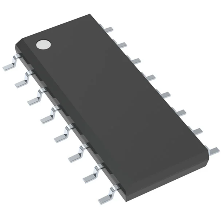
MAX3232 Pinout and CAD Model
MAX 3232 Pin Configuration (16-Pin DIP/SOIC)
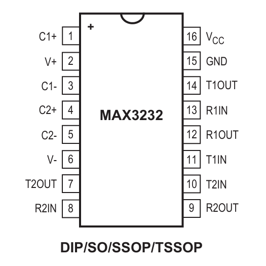
Pin No. | Pin Name | Description |
1 | C1+ | Positive terminal of charge pump capacitor C1 used to generate internal voltages. |
2 | V+ | Positive internally generated voltage from the charge pump (typically around +6V). |
3 | C1- | Negative terminal of charge pump capacitor C1. |
4 | C2+ | Positive terminal of charge pump capacitor C2. |
5 | C2- | Negative terminal of charge pump capacitor C2. |
6 | V- | Negative internally generated voltage from the charge pump (typically around -6V). |
7 | T2 OUT | RS-232 output from transmitter channel 2. |
8 | R2 IN | RS-232 input to receiver channel 2. |
9 | R2 OUT | TTL/CMOS output from receiver channel 2. |
10 | T2 IN | TTL/CMOS input to transmitter channel 2. |
11 | T1 IN | TTL/CMOS input to transmitter channel 1. |
12 | R1 OUT | TTL/CMOS output from receiver channel 1. |
13 | R1 IN | RS-232 input to receiver channel 1. |
14 | T1 OUT | RS-232 output from transmitter channel 1. |
15 | Ground | Ground reference for the device. |
16 | Vcc | Power supply input (3.0V to 5.5V). |
Pin Description Summary
T1 IN / T2 IN → TTL input
T1 OUT / T2 OUT → RS-232 output
R1 IN / R2 IN → RS-232 input
R1 OUT / R2 OUT → TTL output
C1+, C1−, C2+, C2− → External charge pump capacitors
V+ and V− → Generated internal voltages
Vcc → 3.0V–5.5V supply
GND → Ground
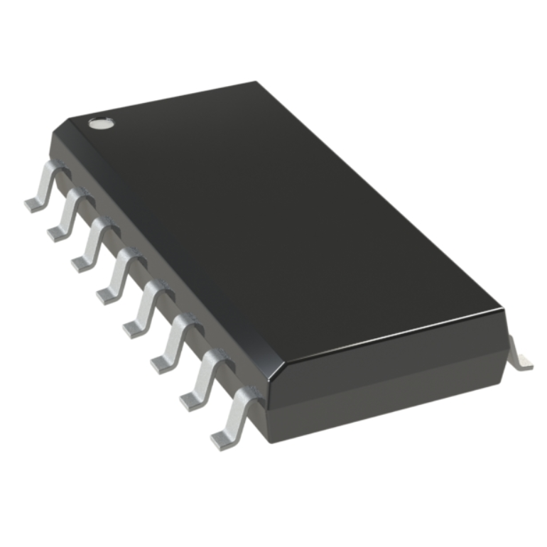
MAX3232 CAD Model
IC MAX3232 Features and Specifications
Integrated Features Save Board Space and Simplify Design
Combines drivers, receivers, and charge pump circuitry in one chip, reducing external components and simplifying PCB layout.
Charge Pump Circuitry Eliminates the Need for a Bipolar ±12V Supply
Generates required RS-232 voltages internally, removing the need for a dual power supply.
Wide Single-Supply Operation From +3V to +5.5V
Works with both 3.3V and 5V systems, making it suitable for modern microcontrollers.
Always-On Extra Outputs Enable Monitoring of External Devices
Receiver outputs stay active, allowing continuous signal monitoring and status detection.
Power Saving Extends Battery Life
Low power consumption makes it ideal for portable and battery-powered devices.
Specification
Parameter | Specification |
Device Type | RS-232 Transmitter/Receiver |
Drivers / Receivers | 2 Drivers, 2 Receivers |
Supply Voltage | 3.0V to 5.5V |
Data Rate | Up to 120 kbps |
Logic Input Level | TTL / CMOS Compatible |
RS-232 Output Voltage | Approximately ±5V to ±6V |
Charge Pump Capacitors | 4 × 0.1µF (external) |
Operating Temperature | −40°C to +85°C (typical industrial range) |
ESD Protection | ±15kV (HBM typical) |
Power Consumption | Low quiescent current operation |
Package Options | DIP-16, SOIC-16, TSSOP-16 |
Communication Mode | Full-duplex serial communication |
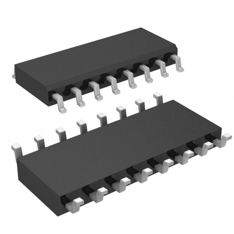
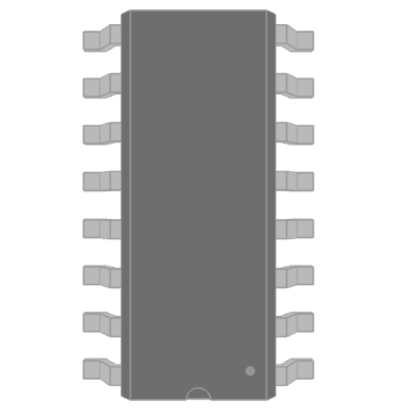
MAX3232 Package Options
Common types:
DIP-16
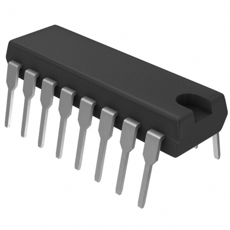
SOIC-16
TSSOP-16
MAXIM MAX3232 Manufacturer
Originally developed by Maxim Integrated, now part of Analog Devices.
MAX 3232 Applications
Battery-Powered Equipment
Low power operation makes it suitable for portable and battery-operated devices.
Hand-Held Equipment
Compact design supports reliable serial communication in handheld instruments and field tools.
Peripherals
Used to connect microcontrollers with printers, scanners, modems, and other serial peripherals.
Datacom Equipment
Provides dependable RS-232 communication in data terminals and industrial communication systems.
How to Use a MAX3232 Converter IC
Basic Steps:
1. Connect Vcc (3.3V or 5V)
2. Connect GND
3. Add four 0.1µF charge pump capacitors
4. Connect:
MCU TX → T1 IN
MCU RX → R1 OUT
T1 OUT → RS-232 RX
R1 IN → RS-232 TX
Important Notes:
Ensure voltage compatibility (3.3V or 5V logic)
Keep capacitors close to IC pins
Avoid long PCB traces on charge pump nodes
MAX3232 Chip Equivalent
The most common chip equivalent is the MAX232. Both ICs serve the same primary function: converting TTL/CMOS logic-level signals to RS-232 voltage levels and vice versa, enabling communication between microcontrollers and RS-232 devices such as PCs, modems, and serial peripherals.
The MAX232 includes two drivers and two receivers, just like the MAX 3232, and uses internal charge pump circuitry to generate the positive and negative voltages required for RS-232 signaling, eliminating the need for a dual ±12V power supply. Its pin configuration and package types (DIP-16, SOIC-16) are also compatible with MAX 3232 designs, making it a drop-in replacement in many circuits.
The main difference is in the supply voltage and target applications. MAX232 is designed primarily for 5V systems, which was standard for older microcontrollers and legacy electronics. In contrast, MAX3232 supports a wider voltage range of 3.0V to 5.5V, making it suitable for modern low-voltage systems, including 3.3V microcontrollers.
Overall, if a circuit originally uses MAX3232, can often use a MAX232 in designs where the system voltage is fixed at 5V. However, for 3.3V systems, prefer the MAX 3232 because proper voltage compatibility and reliable RS-232 output levels. Both chips remain popular in embedded systems, industrial equipment, and serial communication modules.
SP3232 vs MAX3232 vs MAX232
Feature | SP3232 | MAX3232 | MAX232 |
Brand | Sipex | Maxim Integrated | Maxim Integrated |
Supply Voltage | 3.0V~5.5V | 3.0V~5.5V | 5V only |
Data Rate | Up to 250 kbps | Up to 120 kbps | Up to 120 kbps |
Drivers / Receivers | 2/2 | 2/2 | 2/2 |
Charge Pump | Yes | Yes | Yes |
Logic Compatibility | TTL / CMOS | TTL / CMOS | TTL / CMOS |
Operating Temperature | −40°C to +85°C | −40°C to +85°C | −40°C to +85°C |
Package Options | DIP-16, SOIC-16 | DIP-16, SOIC-16, TSSOP-16 | DIP-16, SOIC-16 |
Special Features | High-speed operation | Wide voltage range, low power | Legacy 5V systems, widely available |
Typical Applications | Embedded systems, handheld devices | Modern micro controllers, portable devices | Older PCs, legacy serial devices |
Summary:
MAX232 → Original, 5V only, widely used in older systems.
MAX3232 → Modern replacement, supports 3.3V and 5V systems, low power.
SP3232 → High-speed alternative with wider data rate, compatible with MAX3232 systems.
Datasheet MAX3232 PDF
If you need the complete electrical characteristics, refer to the official Data sheet PDF for detailed timing diagrams and application notes.
MAX3232 RS232 to TTL Serial Port Converter Module Board
The module use the MAX3232 IC, which handles RS-232 to TTL/CMOS voltage level conversion efficiently.
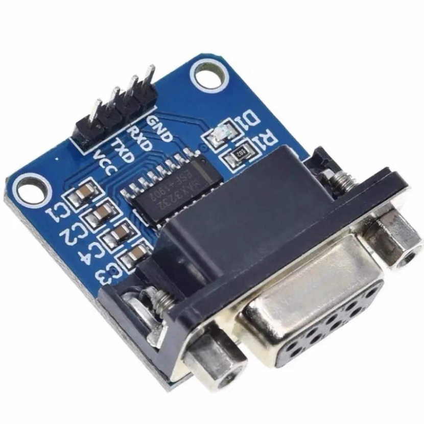
Working Voltage
It operates over a wide voltage range of 3.3V to 5.5V, making it compatible with most modern microcontrollers.
Interface
The board provides TX, RX, VCC, and GND pins for easy connection to microcontrollers and other TTL devices.
Supported Microcontrollers
It works with STC, STM32, NXP, Renesas, and NEC microcontrollers, enabling easy programming and serial communication.
Features
The module is compact, easy to use, and requires no additional circuitry. It supports full-duplex communication, stable RS-232 voltage levels, and low power operation, making it ideal for portable and battery-powered projects.
Applications
The module widely use for radio modification and upgrades, mobile phone flashing, XBOX360 firmware updates, GPS communication, automotive diagnostics, DVD flashing, hard disk repair, and set-top box firmware upgrades.
Frequently Asked Questions [FAQ]
What is MAX3232 used for?
Use to convert TTL/CMOS logic-level signals to RS-232 voltage levels and vice versa, enabling reliable serial communication between microcontrollers, PCs, modems, GPS modules, and other RS-232-compatible devices in embedded and industrial applications.
What is the difference between MAX232 and MAX3232?
MAX232 operates only at 5V supply, while MAX3232 works from 3.0V to 5.5V. MAX3232 is compatible with modern 3.3V microcontrollers and offers low-power operation, whereas MAX232 is designed for legacy 5V systems.
What is the voltage of MAX3232?
The MAX 3232 operates from a single supply voltage between 3.0V and 5.5V. Internally, it generates approximately ±6V using a charge pump to meet RS-232 signaling standards without requiring an external dual-voltage supply.
What does the MAX232 chip do?
The MAX232 converts TTL or CMOS logic-level signals to RS-232 voltage levels and vice versa. It allows microcontrollers or other low-voltage devices to communicate with RS-232 ports on computers, modems, or serial peripherals.
What is the difference between RS-232 and MAX232?
RS-232 is a serial communication standard defining voltage levels, timing, and protocol. MAX232 is an integrated circuit that converts logic-level TTL/CMOS signals into RS-232 compliant voltages for proper communication with RS-232 devices.
What is the price of MAX3232?
The pricing of MAX 3232 varies by package, supplier, and quantity, typically ranging from $0.20 to $2 per unit in bulk orders, and slightly higher for single-piece retail purchases.
What is RS232 to TTL converter?
An RS232 to TTL converter is a module or circuit that translates RS-232 voltage signals (±12V) into TTL/CMOS logic levels (0-3.3V or 0-5V) and vice versa, enabling communication between microcontrollers and RS-232 devices.
Conclusion
The MAX3232 remains one of the most reliable and widely used RS-232 interface ICs in embedded systems. With its wide voltage range, minimal external components, internal charge pump, and strong compatibility with MAX232 designs, it continues to be a preferred solution for serial communication projects.
Whether you’re designing industrial equipment, battery-powered devices, or a simple UART debugging interface, the MAX 3232 provides a stable and efficient RS-232 to TTL conversion solution.
Read More:
1. MAX232 IC: Datasheet, Features, Applications, and Pinout
HOT NEWS
Understanding A 0603 Resistor
0603 resistor,dimensions,marking code, values
2025-05-29
LR41 Battery Guide: Specifications, Equivalents, and Uses
LR41 Battery Specifications, Equivalents, and Uses
2025-12-14
The 0402 Resistor: A Comprehensive Guide
0402 Resistor
2025-05-06
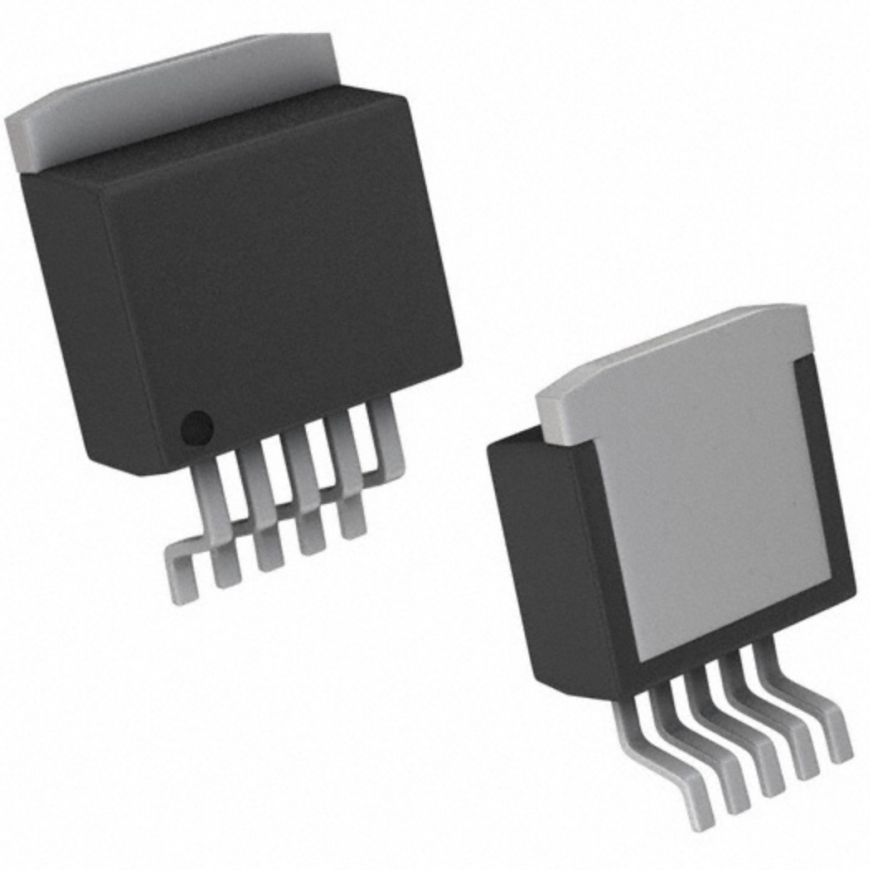
MT3608 Boost Converter - An In-Depth Guide
MT3608 Boost Converter
2025-09-04
What Is A 1206 Resistor?
1206 resistor dimensions,footprint,value
2025-06-05
TP4056 Charging Module Pinout, Working, and Applications
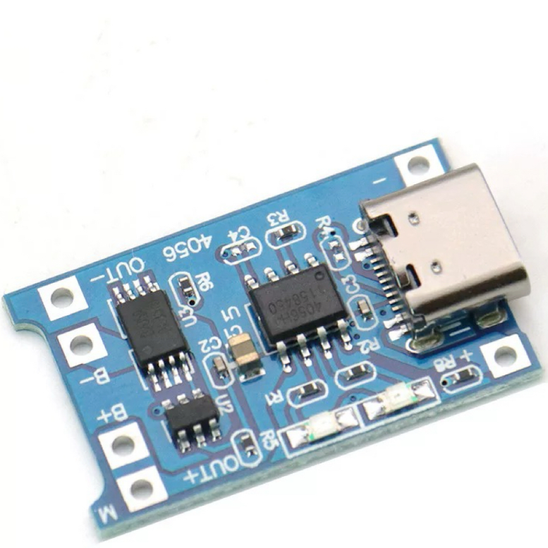
TP4056 Charging Module Pinout, Working, and Applications
2026-01-23
Everything You Need To Know About ARE1309 Relay

2025-04-23
Complete Guide to the 220 Ohm Resistor
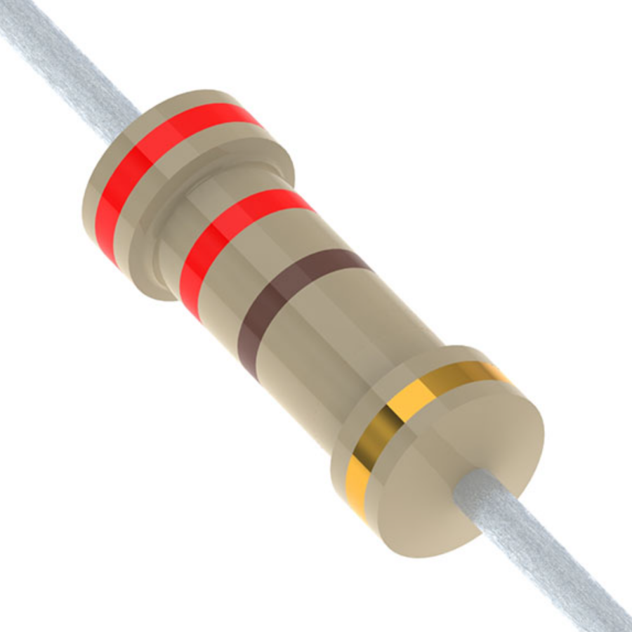
220 Ohm Resistor
2025-07-28
120 Ohm Resistor- Specifications, Applications, and Features
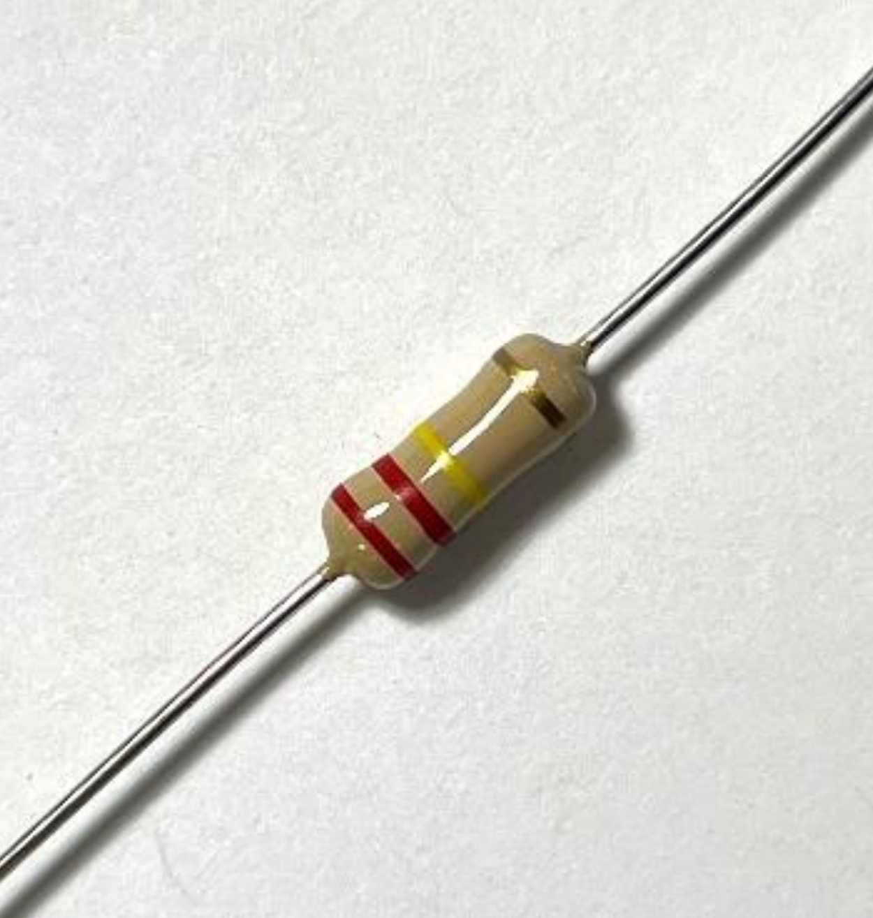
2025-05-12
Guide To The XL6009 Boost Converter
XL6009 Boost Converter
2025-09-05