


 BOM
BOM Cart
Cart Product Catalog
The MT3608 is a highly efficient, current-mode step-up converter widely use in various small, low-power applications. This chip operates with an input voltage range of 2V to 24V, making it suitable for devices powered by batteries or other low-voltage sources. Capable of boosting the input voltage up to 28V, the MT3608 is ideal for projects that require efficient, compact, and versatile voltage conversion.
2. MT3608 Datasheet Specifications
3. MT3608 Symbol, Pinout and Configuration
5. MT3608 Boost Converter Operating Principle
6. Series Connection of MT3608 Chip
9. Frequently Asked Questions [FAQ]
What is a MT3608?
A 6-pin SOT23-6 current mode boost converter design for applications requiring a small form factor and high efficiency. It is a fixed-frequency, peak current mode boost converter that uses an internal 80mΩ MOSFET to reduce switching losses and increase efficiency, allowing the use of small external components such as low-profile inductors and capacitors. At its core, the chip converts lower input voltages (e.g., from a battery) to higher output voltages, maintaining the power required for the operation of various electronic components and systems. This feature makes it indispensable in applications where require space and power efficiency.
MT3608 Alternative and Equivalent
While this chip widely use for low-power step-up conversion, there are several alternatives and equivalents available in the market that offer similar functionality. These substitutes may vary in terms of features such as input/output voltage range, current limits, efficiency, and other performance characteristics. Below are a few similar circuits:
MT36291
Another step-up (boost) converter that provides a similar voltage conversion range and efficiency, making it a viable alternative to the MT3608 in various low-power applications. Typically in SOT23-6 package. The MT36291 feature slight differences in switching frequency, power handling, or efficiency, depending on the specific needs of a design.
SX1308
A compact, low-cost DC-DC step-up converter that operates at a frequency of about 1.2 MHz, similar to the MT3608, and offers high efficiency, typically above 90%. Use for low current applications and can commonly find in small power supply circuits, low-power sensors, and battery-powered devices. While the SX1308 offers a similar voltage conversion range, it might not have the same extensive protection features like thermal overload and current limiting that the MT3608 provides.
LP6238B6F
A high-efficiency step-up converter with a built-in MOSFET, offering smooth operation and efficiency in power conversion applications. Typically use in applications such as LCD bias supplies, battery-powered systems, and portable devices. This alternative may provide different switching characteristics or efficiency but remains a viable replacement for low-power step-up conversion needs in small electronics.
LN2220PAR
Another step-up converter available in small, compact packages SOT23-6. Similar to the MT3608, it provides efficient voltage step-up functionality, but there are slight differences in switching frequencies, efficiency, or other features, depending on specific use cases and requirements.
These alternatives differ slightly in terms of switching frequencies, efficiency, or current limits, but they all offer the same fundamental functionality of boosting low input voltages to higher output voltages.
MT3608 Datasheet Specifications
Aerosemi MT3608 Manufacturer Information
This chip is a step-up converter manufactured by Aerosemi, a company specializing in power management integrated circuits (ICs). Aerosemi designs efficient, compact, and reliable power conversion solutions suitable for various applications, including low-power, battery-operated devices. The MT3608 is one of their key offerings in the category of DC-DC boost converters, design to provide high efficiency and a small footprint, making it ideal for space-constrained applications.
Key Electrical Specifications
Input Voltage Range: 2V to 24V
Output Voltage: Adjustable up to 28V
Switching Frequency: 1.2 MHz (fixed frequency)
Efficiency: Up to 93%
Maximum Output Current: 2A
Current Limit: 4A (internal protection)
Thermal Shutdown Protection: Yes
Under-voltage Lockout: Yes
Soft-Start: Yes, for reduced inrush current
Ripple Voltage: Low, typically under 50mV
Operating Temperature Range: -40°C to 85°C
MT3608 Characteristics
Characterize by its current-mode control architecture, providing precise regulation of the output voltage. Its main features include:
Small Footprint, comes in a 6-pin SOT23-6 package, which is small and efficient for integration into space-constrained designs. High Efficiency up to 93%, the circuit ensures minimal energy loss, which is necessary in battery-powered applications. Automatic Pulse Frequency Modulation (PFM) at Light Loads, This helps in reducing power consumption at low output powers levels. Built-in Protections, features include overcurrent and thermal overload protection, under-voltage lockout to safeguard the circuit in case of fault conditions. Soft-Start Function: This ensures that the device gradually reaches operating conditions, reducing stress on the components and extending the life of the battery.
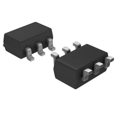
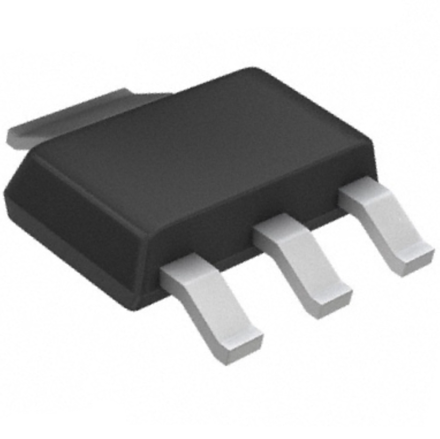
Packaging: SOT23-6
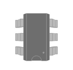
A 6-pin SOT-23-6 package, which is a small surface-mount device (SMD) package. This package is known for its compact size, making it ideal for integration into portable and low-power devices where space is limited. The small form factor of the SOT-23-6 packages make it easy to integrate into modern PCB designs, allowing for efficient use of space and providing low-profile solutions for electronics projects.
Product Category
The chip falls under the DC-DC Converters category, specifically as a boost converter. Boost-converters use to step up (increase) the voltage from a lower input to a higher output voltage, making them useful in various applications such as:
battery-powered electronics, power supply for small devices, portable gadgets, set-top boxes, networking device and LCD bias supplies.
The circuit is also classified under Power Management ICs (PMICs), a category that includes devices responsible for efficiently managing power flow and energy conversion in electronic circuits.
The MT3608 PDF datasheet contains the full technical details, including recommended operating conditions, application notes, and recommended external components.
MT3608 Symbol, Pinout and Configuration
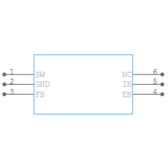
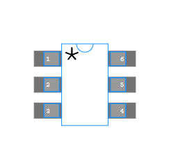
Understanding the chip pinout is necessary for integrating it into your circuits. The 6-pin package configuration design for easy use with minimal external components. Below is the breakdown of the pins, which outlines the specific functions of each pin in the device.
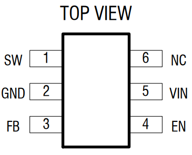
Pin Description:
Pin 1: SW (Power Switch Output)
The SW pin is the output of the internal MOSFET switch and is the key node where power deliver to the load. It connects to the inductor and output rectifier in the boost converter circuit. The voltage at the SW pin can fluctuate between GND and 28V, depending on the feedback and the input voltage. When the converter is operating, this pin switches between on and off states, effectively controlling the energy transfer to the output. The SW pin is useful because it governs the step-up function of the converter, which boosts the input voltage to a higher, regulated output voltage.
Pin 2: GND (Ground Pin)
The GND pin serves as the common reference point for the entire converter. It is the ground for both the input and output circuits and helps establish a shared voltage reference for the operation of the device. Proper grounding is necessary for stable operation and minimizing noise in the circuit. All other pins in the chip reference to this ground pin, and it plays a role in ensuring accurate voltage regulation and safe operation.
Pin 3: FB (Feedback Input)
The FB pin is the feedback input that plays a central role in voltage regulation. The circuit uses a feedback loop to adjust the output voltage. The voltage at FB is internally regulated to 0.6V, which is the reference voltage. To set the desired output voltage, connect a resistor divider network to this pin. Compare the feedback voltage at FB to the reference voltage, and the converter adjusts the duty cycle of the internal MOSFET to maintain the output voltage at the desired level. This feedback mechanism ensures that the output voltage remains stable, even as input conditions or load requirements change.
Pin 4: EN (Enable Pin)
The EN (Enable) pin controls whether the converter power on or off. When apply a high voltage to this pin, the converter is enabled and starts operating. When apply a low voltage, the device is disabled and goes into a low-power state. In many applications, connect the EN pin directly to the input supply voltage, which allows the converter to automatically start when apply the input voltage. Alternatively, can use a control signal to manage the operation of the converter, providing flexibility for system design.
Pin 5: VIN (Input Supply Pin)
The VIN pin is where the input voltage supply to the converter. This pin must be properly bypassed with capacitors (typically ceramic capacitor) to reduce noise and ensure stable operation. The input voltage must fall within the specified range of 2V to 24V to ensure proper functionality. The chip will step up this input voltage to a higher output voltage, depending on the feedback control at the FB pin. Proper filtering at the VIN pin helps minimize high-frequency noise and prevents instability in the MT3608's operation.
Pin 6: NC (No Connect)
The NC pin, short for No Connect, does not require any electrical connection. It is typically left floating or unconnected in a circuit design. The presence of this pin is simply for package design reasons and does not affect the performance of the converter. It is important to ensure that NC is not accidentally connected to ground or any other voltage source, as this could lead to unintended circuit behavior or malfunctions.
By understanding the converter pinout and correctly wiring the pins, designers can take full advantage of the converter’s features, ensuring a reliable and efficient voltage boost for various low-power applications. Whether use for battery-powered sensors, small gadgets, or low-power power supplies, the converter provides a flexible, high-efficiency solution with easy integration into compact designs.
MT3608 Pros and Cons
This chip is a popular DC-DC step-up (boost) converter known for its compact size, high efficiency, and ease of integration into low-power designs. However, like all electronic components, it comes with both advantages and limitations that must consider depending on the application. Below is a breakdown of the pros and cons of the circuit.
Pros:
1. High Efficiency (Up to 93%)
One of the standout features is its high efficiency, which can reach up to 93%. This means less energy waste as heat, making the device ideal for battery-powered applications where every bit of power counts. High efficiency also results in longer battery life, which is useful for portable electronics.
2. Compact Package (SOT23-6)
The 6-pin SOT23-6 package, which is small and lightweight, making it perfect for space-constrained designs. The compact size allows it to integrate into various applications without occupying much PCB space, which is beneficial in modern, miniaturized devices.
3. Wide Input Voltage Range (2V to 24V)
Provides flexibility, allowing the chip to use in a wide variety of power sources, from low-voltage batteries to higher DC supplies. This makes it versatile for use in many types of electronic projects.
4. Internal Protection Features
The converter comes with built-in thermal overload protection, overcurrent protections, and under-voltage lockout. These protection mechanisms ensure that the converter operates safely, preventing damage to the device and connected components in the event of an overload or fault conditions.
5. Soft-Start Function
The feature reduces the inrush current when the device power on. This prevents excessive stress on the power supply and reduces the chances of damaging sensitive components. The soft-start function also helps to minimize voltage spikes during startup.
6. Pulse Frequency Modulation (PFM) Mode at Light Loads
The converter automatically shifts to pulse frequency modulation (PFM) mode under light load conditions. This reduces power consumption and improves overall efficiency at low output power levels. It makes the device more energy-efficient in applications where the load can vary.
7. Adjustable Output Voltage
The chip can adjust output voltages, allowing it to configure for different voltage levels based on the application. The output voltage can be set up to 28V, making the converter versatile for a range of applications requiring various voltage outputs.
Cons:
1. Limited Output Current (2A)
While the chip is efficient, its output current is limited to 2A. This makes it less suitable for applications that require higher output currents, such as high-power devices, large motors, or high-current LEDs. For such use cases, a converter with a higher current rating would be necessary.
2. No Reverse Voltage Protection
This meaning that if connect the input voltage with reversed polarity, the device can damage. External protection circuits are necessary to safeguard the device against reverse voltage situations.
3. Temperature Sensitivity at High Loads
Under high load conditions, the chip may generate heat, especially when delivering close to its maximum output current of 2A. Thermal management is necessary to ensure the device doesn’t overheat, and need additional cooling solutions (such as heat sinks) for applications with higher power requirements.
4. No Integrated Output Capacitor
The chip requires external capacitors for stable operation. While this allows for flexibility in choosing capacitor values, it also means that designers must take care to select the appropriate components to ensure optimal performance and avoid instability.
5. Limited Input Voltage Range at High Efficiency
Although the input voltage range is quite broad (2V to 24V), the MT3608's maximum efficiency is typically achieved when the input voltage is closer to the higher end of the range. When operating at low input voltages, the efficiency may drop, especially under higher output currents.
6. Limited Protection Features
While the converter includes basic protection features, it lacks some advanced protection features found in other converters, such as overvoltage protection. This may be a concern in critical applications where require additional fault tolerance.
MT3608 Boost Converter Operating Principle
This chip works as a current-mode boost converter, utilizing an internal MOSFET switch to step up the input voltage. The converter works by storing energy in an inductor when the MOSFET is on and transferring that energy to the output capacitor when the MOSFET is off. A feedback control loop ensures the output voltage remains regulated.
The peak current mode control prevents sub-harmonic oscillations at high duty cycles, ensuring stable operation. Internal soft-start limits inrush current during startup, helping extend the battery life in portable applications.
Functional Description:
1. Fixed Frequency Operation
Operate at a fixed switching frequency of 1.2 MHz. This frequency determines how often the internal MOSFET switch on and off, allowing for efficient energy conversion. The fixed frequency helps maintain consistent operation, making it easier to design systems with predictable behavior.
2. Peak Current Mode Control
At the start of each cycle, the MOSFET turn on by the control circuitry. The primary goal is to regulate the output voltage by adjusting the peak current of the inductor. Peak current mode control monitors the inductor's current, using it as feedback to control the timing of the MOSFET switching.
3. Prevention of Sub-Harmonic Oscillations
When the duty cycle (the ratio of on-time to off-time of the MOSFET) exceeds 50%, there is a potential for sub-harmonic oscillations. To prevent this instability, the converter adds a stabilizing ramp to the output of the current sense amplifier. This ramp is fed into the negative input of the PWM (Pulse Width Modulation) comparator.
4. PWM Control and Output Regulation
The PWM comparator compares the voltage from the current sense amplifiers (with the stabilizing ramp) to the voltage from the error amplifier. The error one outputs a voltage that is an amplified version of the difference between the 0.6V bandgap reference voltage and the feedback voltage at the FB pin. This regulation ensures that the output voltage remains stable, even when there are fluctuations in load or input voltages.
5. Regulation of Output Voltages
When the voltage at the FB pin drops, the error amplifier increases its output. This increase in the error amplifier's output drives the control circuitry to allow more current to flow through the MOSFET. As a result, more energy transfer to the output, increasing the output-voltage. This dynamic feedback loop ensures that the output voltage remains regulated under varying load conditions.
6. Current Limiting and Protection
The current limiting to prevent damage in case of an overload. If the output voltage or current exceeds safe operating levels, the internal protection mechanisms will step in to either shut down or limit the output to safe levels, preventing damage to the device and external components.
Series Connection of MT3608 Chip
In certain applications, it is necessary to connect multiple boost converters in series to meet higher voltage requirements or achieve a higher output voltage than a single converter can provide. However, connecting multiple chips in series is not a typical application for this boost converter, as they design to step up a low voltage to a higher voltage with a single unit. Instead, in most cases, parallel configurations or stacking converters are more commonly use to meet current requirements.
That said, if you were to connect multiple chips in series, you would generally need to consider the following points:
1. Voltage Scaling
When connecting chips in series, the output voltage of each converter would add up, allowing for a higher combined voltage. For example, two MT3608s, each producing 12V, would yield an output of 24V when connected in series. The principle here is the same as with batteries connected in series, where the voltages add up, but the current remains the same as with a single converter.
However, to ensure proper voltage control and stability across the series-connected converters, you'd need to:
Ensure each converter properly regulate to avoid excessive voltage buildup that could damage the devices.
Carefully control the feedback to ensure each converter maintains an appropriate output voltage without causing instability in the system.
2. Feedback Loop Issues
Since each converter has its own feedback loop based on the FB pin, it could be challenging to synchronize the output voltage regulation when connecting in series. Normally, the feedback loop design to regulate a single output voltage. When use in series, each converter may try to regulate its own voltage without considering the others, leading to inconsistent regulation or voltage imbalance.
To mitigate this:
You would need to synchronize the FB pins of the converters, which could involve using a common feedback voltage reference for the series-connected MT3608s.
Alternatively, you might need to use external control circuitry to regulate the feedback and ensure all converters operate harmoniously, which could involve complex design.
3. Current Limitations
Since the chip is a current-mode boost converter, the current output remains the same as the rated output current of a single converter, typically around 2A. In a series connection, while the voltage will add up, the current capacity will not increase. For applications requiring higher current, a series connection would not inherently provide more current; each converter would still only supply the current limited by its internal circuitry.
To achieve higher current outputs, you would need to consider:
Parallel connections of chips, where each converter operates independently to supply the same output voltage, but share the total current load.
Using a current-sharing circuit for parallel converters to ensure that the current distribute evenly between them.
4. Protection Considerations
When connecting MT3608s in series, proper over-voltage protection and current limiting must be in place to prevent damage to the devices. The circuit does include internal protection features such as overcurrent protection and thermal shutdown, but these might not be effective in a series configuration if the converters are not properly synchronized.
To ensure safe operation:
Use diodes to protect each chip from reverse current or unexpected voltage surges.
Include fuse protection in each output to safeguard against overloads or faults.
5. Practicality and Use Cases
Typically, not recommend series connections of boost converters are unless for very specific and high-voltage applications, as they would require significant external circuitry to synchronize feedback, protect from overvoltage, and manage current. Most applications requiring high output voltages are better suited to using higher-rated boost converters, such as the XL6009 or LT3750, or employing series-connected battery systems.
Alternative Approach: Parallel Configuration
Instead of connecting chips in series, a more common and practical approach for increasing current output is to connect multiple MT3608 converters in parallel. This allows the current capacity to scale up while keeping the voltage regulated. In such cases:
Each converter will output the same voltage, but the total output current will increase.
You need to ensure proper current-sharing between the parallel converters, either by using an appropriate design for current distribution or using a master-slave configuration with one chip controlling the others.
MT3608 Application
This boost converter is highly versatile and can use in a wide range of applications, particularly where require efficient voltage boosting for battery-powered devices or other low-power electronic circuits. Below are some common and potential applications:
1. Commonly use in battery-powered devices that require a higher output voltage than the input. Since it operates efficiently and consumes low power, it’s perfect for portable electronics, such as:
Handheld devices (e.g., portable sensors, meters, and gadgets).
Wireless devices (e.g., Bluetooth speakers, wireless charging circuits).
Power supplies for small devices such as cameras or wearable electronics.
Its high efficiency ensures that extend battery life, which is crucial in battery-operated systems.
2. Use in set-top boxes (STBs) for television and media streaming, can employ the converter to boost the input voltage to the required level for powering various internal components. These devices often rely on compact power management solutions that maintain efficiency while delivering the required voltage, which makes the circuit a good fit as its small form factor and high efficiency.
3. Ideal for LCD bias supplies, which require a regulated, stable voltage. LCD screens need a high and stable bias voltage to operate effectively, particularly in portable devices such as smartphones, tablets, and wearable displays. The chip can efficiently step up the low voltage from the battery or input power to the higher voltage needed for biasing the LCD.
4. DSL modems, cable modems, and routers often require a step-up converter to power their internal circuits from a relatively low DC input, typically from a USB power supply or lower-voltage power adapters. The MT3608’s small size and high efficiency, is perfect for these devices, ensuring they run efficiently without requiring bulky power supplies.
5. In networking cards, particularly those powered through PCI or PCI Express (PCIe) slots, can use to step up the 5V or 3.3V provided by the slot to the required voltage for the card’s internal components. Networking cards, such as Ethernet or wireless cards, often require stable and higher voltages for signal processing and other functions, making it ideal for this application.
The dc converter can also use in various other applications where need small, efficient, and reliable voltage boost converters, such as:
Portable charging circuits.
LED drivers for low-power applications.
Solar power systems where the voltage needs to boost from a low level to power devices.
Small power supplies for microcontrollers and other low-voltage circuits.
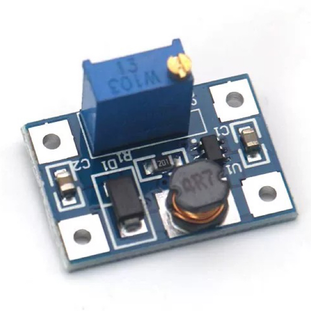
MT3608 Board Boost module
The boost converter is available in several board configurations that provide different types of input and output options, making it highly versatile for various applications. Below are descriptions of three popular MT3608-based board boost modules, which offer step-up functionality with adjustable output voltage and different input methods (USB, Type-C):
MT3608 DC DC Step up Converter 2A 5V to 12V Adjustment
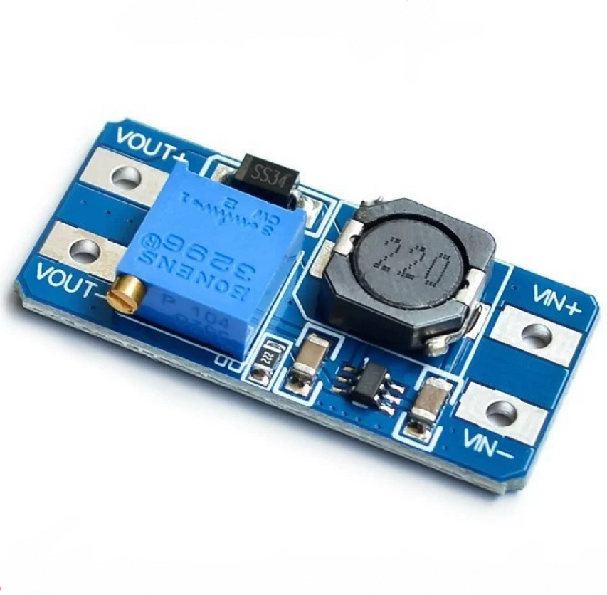
This version board allows you to step up a 5V input to an adjustable 12V output, with a current capability of up to 2A. This module widely use for applications that require a stable, regulated 12V output from a 5V source, such as powering small devices that need 12V but only have access to a 5V source, like Arduino or Raspberry Pi projects that require 12V for peripherals such as motors, LED strips, or servos. It also serves as a power source for low-power electronics that need to drive with higher voltages for specific functions. The module includes an adjustable potentiometer to fine-tune the output voltage from 5V to 12V, and a compact form factor making it suitable for integration into space-constrained designs.
MT3608 DC-DC Boost Converter with Micro USB
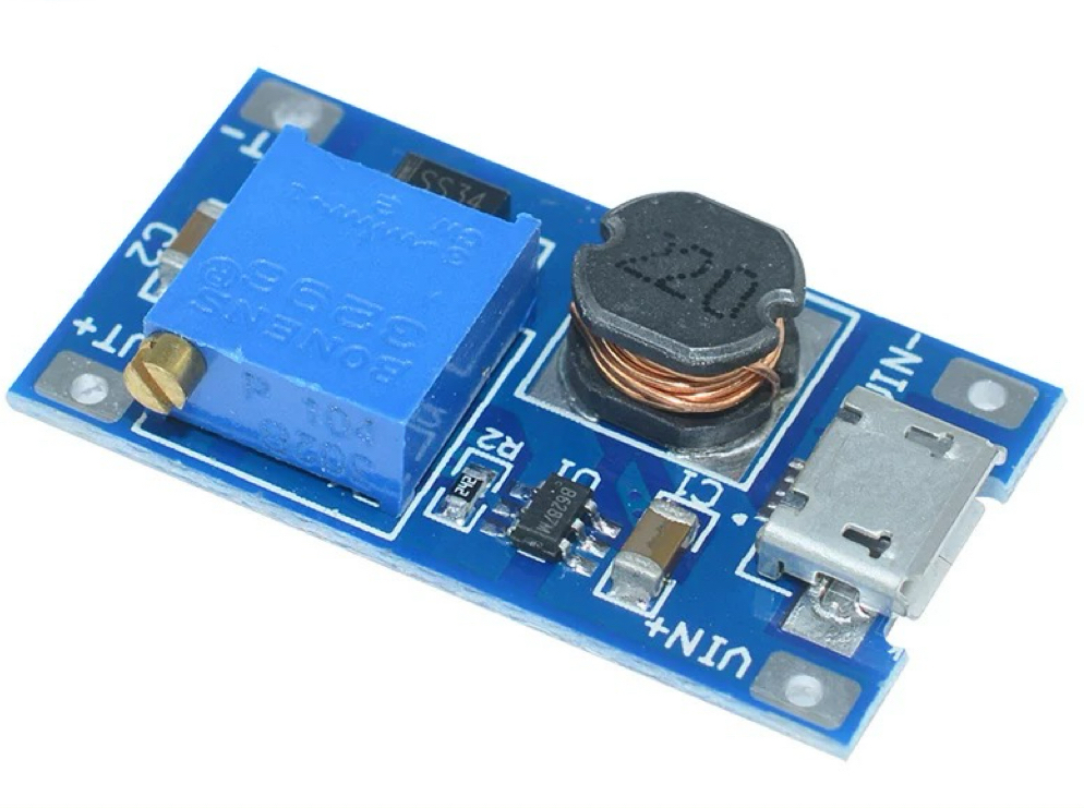
This board comes with a micro USB input port, allowing it to power directly from USB sources such as a USB charger, power bank, or computer USB port. It still offers the adjustable output from 5V to 12V, similar to the previous module, but with the added convenience of the USB input. This is particularly useful for projects that require portability and USB compatibility. With micro USB input is ideal for portable power supplies that step up 5V USB power from a power bank to a higher voltage (e.g., 12V for powering small appliances or LED strips). Also commonly use in prototyping and DIY projects where USB power is available but require a higher output voltage, such as battery charging circuits that use USB input to charge devices needing 12V.
MT3608 DC-DC Step-Up Converter with Type-C
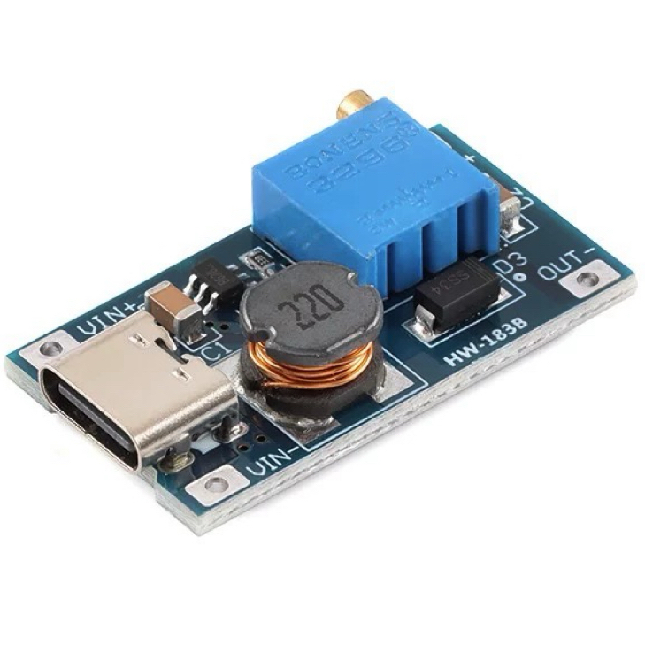
With the Type-C input is similar to the micro USB version but uses the more modern Type-C port for power input. USB Type-C is increasingly popular as its reversible plug, higher power capacity, and faster data transfer capabilities. This module allows users to step up a 5V input from Type-C sources to an adjustable 12V output, with a maximum current of 2A. It's perfect for applications involving modern USB Type-C powered devices such as laptops, smartphones, and power banks that use Type-C for power delivery. Ideal for higher power applications where prefer USB Type-C for its durability and power transfer capabilities. Additionally, it's use in portable electronics and DIY projects requiring a regulated 12V from USB Type-C sources.
Summary of Key Differences
Feature | DC-DC (5V to 12V) | DC-DC (Micro USB) | DC-DC (Type-C) |
Input | 5V DC | Micro USB (5V) | USB Type-C (5V) |
Output Voltage | 5V~12V (Adjustable) | 5V~12V (Adjustable) | 5V~12V (Adjustable) |
Current Output | 2A | 2A | 2A |
Portability | Moderate (requires 5V DC input) | High (USB-powered) | High (USB Type-C powered) |
Applications | Small devices requiring 12V from 5V | Portable 12V from USB power | Modern USB Type-C powered devices |
Frequently Asked Questions [FAQ]
How to use the MT3608 boost converter?
To use the converters, connect a 5V input to the VIN pin. The GND pin should connect to the ground. For output, connect the desired load to the SW and GND pins. Adjust the output voltage by turning the potentiometer on the board, which allows you to set the voltage from 5V to 12V. The circuit can provide up to 2A of current. Ensure that capacitors use at the input and output for proper filtering. Finally, use the EN pin to enable or disable the converter.
What is mt3608 price and where to buy?
The boost converter typically costs between $0.03~$0.45 depending on the seller and any additional features the module may have (e.g., USB input). You can buy it from online retailers or Electronic component stores. For bulk purchases or for specialized versions of the module, you may want to contact local distributors or manufacturers directly for pricing and availability.
What is the difference between MT3608 and XL6009?
Both are DC-DC boost converters, but the XL6009 has a higher current output capability, typically rated for 4A compared to the MT3608’s 2A. The XL6009 operates at a slightly lower switching frequency (typically around 400kHz), while the MT3608 runs at 1.2MHz, making it more suitable for applications requiring compact, high-frequency operation. Additionally, the XL6009 can support higher input and output voltages (up to 40V), whereas the MT3608’s limited to 28V.
What is the voltage range of MT3608?
The dc converter has an input voltage range of 2V to 24V, making it suitable for a variety of low-voltage sources such as batteries or USB power. The output voltage can adjust between 5V to 28V, depending on the application. This range of output voltage is ideal for powering devices that require higher voltage than the input, such as small motors, sensors, or LED strips, making it versatile for numerous applications in portable electronics, DIY projects, and battery-powered systems.
What is the current limit of MT3608?
The MT3608’s output has a current limit of 2A, meaning it can safely provide up to 2 amperes of current to the connected load. Exceeding this current limit may trigger the internal overcurrent protection feature, potentially causing the converter to shut down or reduce its output to protect the circuit. For applications requiring higher current, a different boost converter with a higher current rating, such as the XL6009 (which supports up to 4A), will be more suitable.
How to connect MT3608?
To connect it, start by connecting the input voltage (usually 5V) to the VIN pin. Ensure the GND pin connect to the common ground of the circuit. Then, connect the load to the SW pin for the output, and also tie the GND of the load to the ground. Adjust the output voltage by turning the potentiometer on the board to the desired level, usually between 5V and 12V. The EN pin controls power, which can be tied to the input supply for automatic startup.
What is the frequency of the MT3608 switch?
The converter operates with a fixed switching frequency of 1.2 MHz. This high frequency allows the use of smaller inductors and capacitors in the circuit, making the converter more compact and efficient. The switching frequency helps determine the size of the components, the efficiency of the conversion, and the noise characteristics of the power supply. The 1.2 MHz frequency is optimal for many low-power applications, offering a good balance between size, efficiency, and noise performance.
What is the difference between LM2596 and MT3608?
Both are DC-DC step-down (buck) and step-up (boost) converters, respectively. The LM2596 is a buck converter design to step down higher voltages, typically from 4V to 40V, to a lower output voltage. Can deliver up to 3A of current. In contrast, the MT3608 is a boost converter design to step up a low voltage (e.g., 5V) to a higher voltage, such as 12V, with a current limit of 2A. The LM2596 typically use in step-down applications, while the MT3608 use for step-up applications.
This comprehensive guide covers the essentials of the MT3608 boost converter, from its specifications and applications to the operation and frequently asked questions. Understanding these details will help you integrate this efficient power management solution into your next project!
Read More:
1. Guide To The AMS1117 Voltage Regulator
HOT NEWS
Understanding A 0603 Resistor
0603 resistor,dimensions,marking code, values
2025-05-29
The 0402 Resistor: A Comprehensive Guide
0402 Resistor
2025-05-06
LR41 Battery Guide: Specifications, Equivalents, and Uses
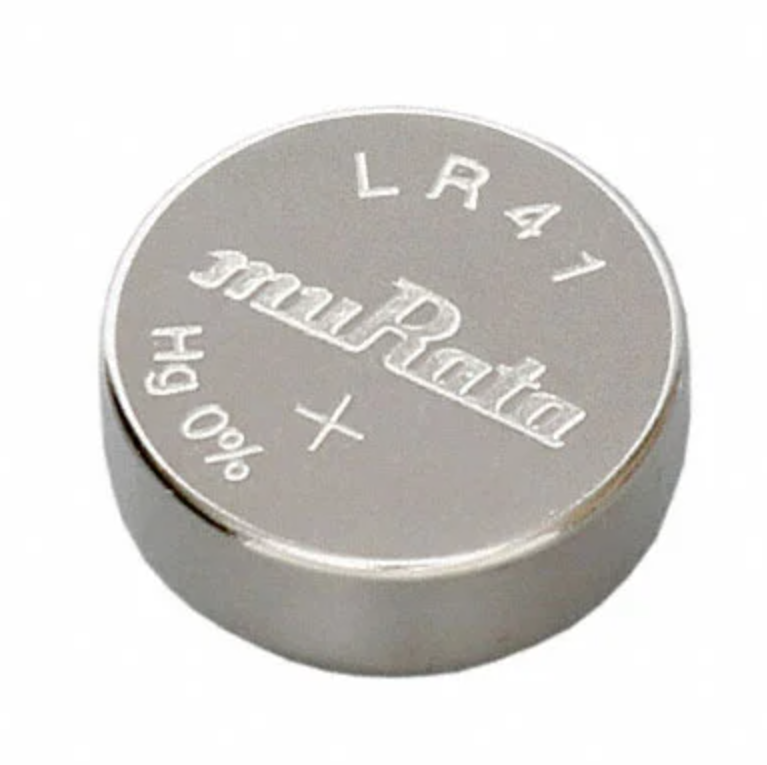
LR41 Battery Specifications, Equivalents, and Uses
2025-12-14
MT3608 Boost Converter - An In-Depth Guide
MT3608 Boost Converter
2025-09-04
What Is A 1206 Resistor?
1206 resistor dimensions,footprint,value
2025-06-05
TP4056 Charging Module Pinout, Working, and Applications
TP4056 Charging Module Pinout, Working, and Applications
2026-01-23
Everything You Need To Know About ARE1309 Relay

2025-04-23
Complete Guide to the 220 Ohm Resistor
220 Ohm Resistor
2025-07-28
120 Ohm Resistor- Specifications, Applications, and Features
2025-05-12
Guide To The AMS1117 Voltage Regulator
AMS1117 Voltage Regulator Circuit
2025-08-17