


 BOM
BOM Cart
Cart Product Catalog
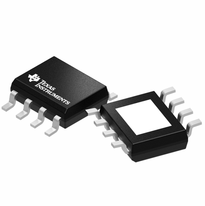
The TPS5430 is a widely used DC-DC step-down (buck) converter IC known for its high efficiency, wide input voltage range, and compact design. Developed by Texas Instruments, commonly find in industrial, consumer, and automotive power supply applications.
This guide walks you through everything you need to know—from working principles and pin configuration to applications, modules, and FAQs.
2. Pinout Configuration of TPS5430
7. TPS5430 Positive Negative Dual Switching Power Supply Module
8. Frequently Asked Questions [FAQ]
What is TPS5430?
The TPS5430 is a high-output-current PWM buck (step-down) converter developed by Texas Instruments. It integrates a low-resistance, high-side N-channel MOSFET, enabling efficient power conversion with minimal external components.
This device includes a high-performance voltage error amplifier, which ensures accurate and stable output voltage even during transient load changes. An undervoltage lockout (UVLO) circuit prevents the converter from starting until the input voltage reaches approximately 5.5V, improving reliability.
To manage startup conditions, the TPS 5430 features an internal soft-start circuit that limits inrush current. Additionally, a voltage feedforward mechanism enhances transient response, allowing the system to quickly adapt to input voltage variations.
The ENA (enable) pin allows the device to enter a low-power shutdown mode, reducing supply current to around 15µA. Other built-in protections include overcurrent limiting, overvoltage protection, and thermal shutdown, ensuring safe operation under various conditions.
To simplify design, the TPS543x family uses internal loop compensation, reducing the need for external components. The TPS 5430 supports input voltages up to 36V and can regulate power from sources such as a 24V bus. It comes in a compact, thermally enhanced 8-pin SOIC PowerPAD package, making it suitable for space-constrained designs.
Additionally, Texas Instruments provides evaluation modules and design tools to help engineers quickly develop high-performance power supply solutions.
Pinout Configuration of TPS5430
The chip comes in an 8-pin PowerPAD™ package designed for thermal efficiency.
Pin Descriptions:
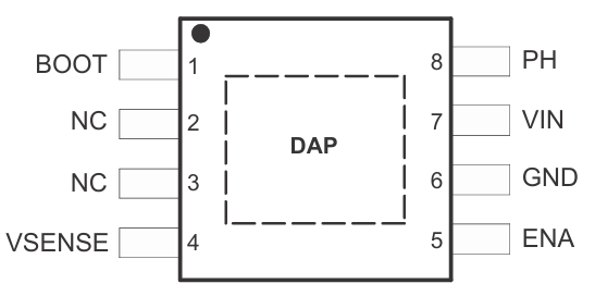
Pin Name | Pin No. | I/O | Description |
BOOT | 1 | O | Boost capacitor for the high-side FET gate driver. Connect a 0.01 µF low-ESR capacitor from BOOT to PH. |
NC | 2, 3 | — | Not connected internally. |
VSENSE | 4 | I | Feedback voltage input for the regulator. Connect to output voltage divider. |
ENA | 5 | I | Enable control pin. Below 0.5V, the device stops switching. Leave floating to enable operation. |
GND | 6 | — | Ground pin. Must connect to PowerPAD for proper operation. |
VIN | 7 | I | Input supply voltage. Bypass to GND with a high-quality low-ESR ceramic capacitor placed close to the IC. |
PH | 8 | I | Switching node (source of high-side MOSFET). Connect to external inductor and diode. |
PowerPAD | — | — | Exposed pad must connect to GND for thermal performance and proper operation. |
Functional Diagram of TPS5430
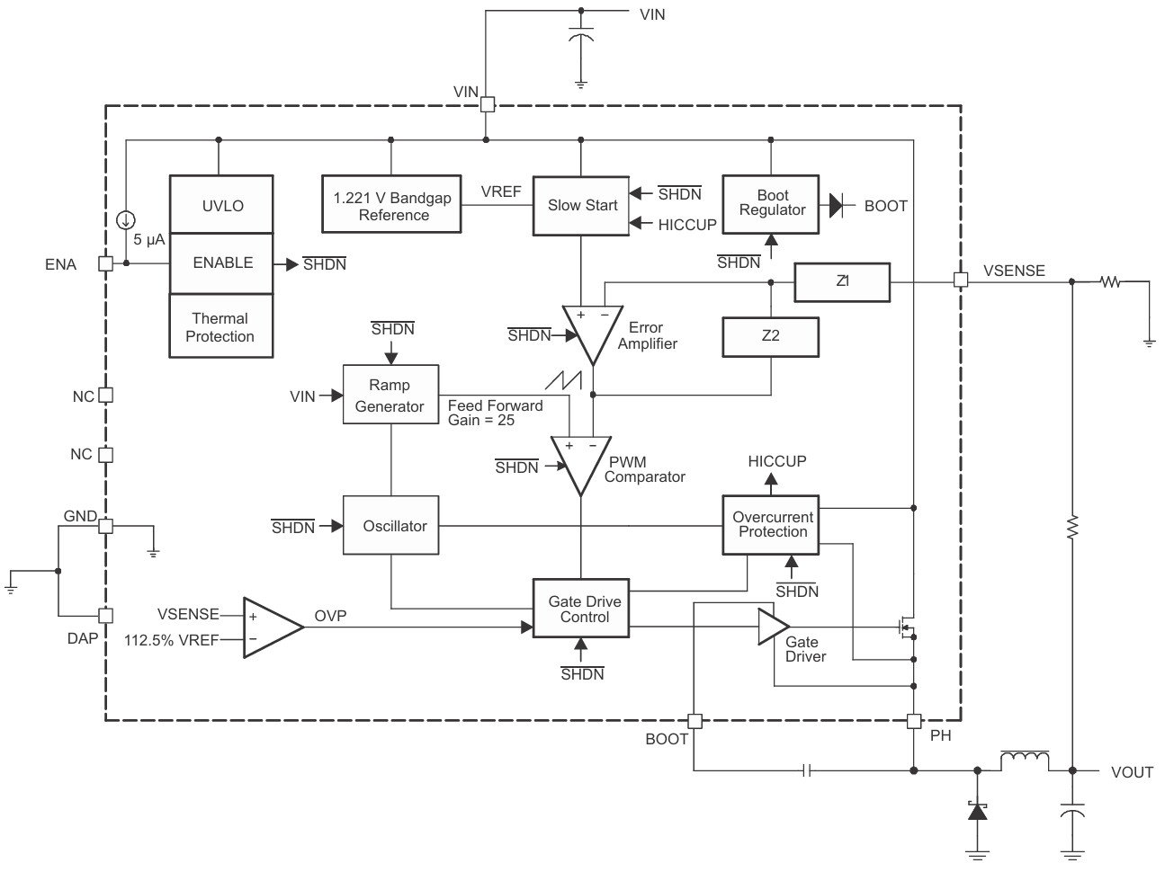
Internally, the chip operates as a fixed-frequency PWM buck regulator (500kHz). It uses: A switching MOSFET to regulate voltage, an external inductor and diode for energy transfer, a feedback loop for output stabilization.
The internal compensation eliminates the need for complex loop design, which is especially helpful for beginners and rapid prototyping.
Detailed Specifications
Table
Parameter | Specification |
Manufacturer | Texas Instruments |
Device Type | Buck Converter |
Topology | PWM (Fixed Frequency) |
Input Voltage Range | 5.5V – 36V |
Output Voltage Range | 1.221V –32.04V |
Output Current | 3A (Continuous), 4A (Peak) |
Switching Frequency | 500kHz |
Efficiency | Up to 95% |
MOSFET Rds(on) | 100mΩ (Typical) |
Reference Voltage | 1.221V |
Feedback Accuracy | ±1.5% |
Quiescent Current | ~15µA (Shutdown Mode) |
Operating Temperature Range | –40°C to 125°C |
Package Type | 8-Pin SOIC PowerPAD™ |
Manufacturer Details
Texas Instruments (TI) is a leading semiconductor company specializing in analog integrated circuits, embedded processors, and power management solutions. The company offers a wide range of products including DC-DC converters, microcontrollers, amplifiers, and sensors, and operates in over 30 countries with a strong global supply chain. TI is well known for its high reliability, long product lifecycle support, and comprehensive design resources such as WEBENCH® Power Designer and evaluation modules, which help engineers accelerate development.
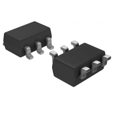
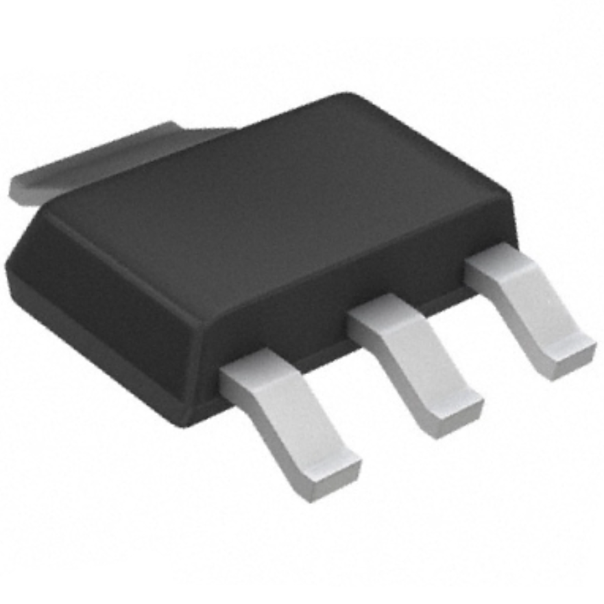
TPS5430 Packaging
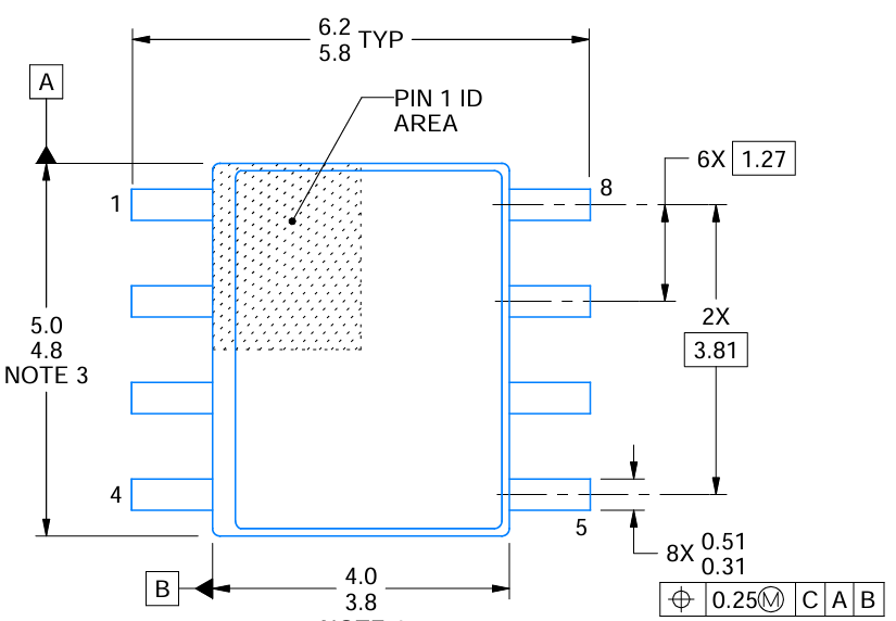
The TPS 5430 is in a compact and thermally efficient package designed for power applications. It is available in an 8-pin SOIC (Small Outline Integrated Circuit) PowerPAD™ package, which integrates an exposed thermal pad on the underside of the device.
This PowerPAD™ must solder directly to the PCB ground plane to improve heat dissipation and ensure stable operation under high load conditions. The compact package size (approximately 3.90 mm width) makes it suitable for space-constrained designs while still supporting up to 3A continuous output current.
The packaging optimize for automated assembly, good thermal performance, and reliable electrical characteristics, making it ideal for industrial, consumer, and embedded power supply applications.
TPS5430 Features
Wide Input Voltage Range
The TPS 5430 supports a broad input range from 5.5V to 36V, making it suitable for 12V, 24V, and industrial power rails.
High Output Current Capability
It provides up to 3A continuous output current and 4A peak current, supporting medium-power DC-DC conversion applications with stable performance under load changes.
High Efficiency Performance
Efficiency can reach up to 95%, thanks to the integrated 100mΩ low-side resistance MOSFET, which reduces conduction losses and improves thermal performance.
Wide Adjustable Output Voltage
Can adjust the output voltage down to 1.22V with 1.5% initial accuracy, allowing flexible use in digital, analog, and mixed-signal circuits.
Internal Compensation
The internal compensation network reduces external component count, simplifying loop stability design and making it easier for engineers to implement.
Fixed Switching Frequency
A fixed 500kHz switching frequency enables the use of smaller inductors and capacitors, helping reduce overall PCB size and cost.
Improved Line and Load Transient Response
The internal voltage feedforward control improves response speed during sudden input or load changes, ensuring better voltage stability.
Built-in Protection Features
The device includes overcurrent limiting, overvoltage protection, and thermal shutdown, providing strong protection against fault conditions and improving system reliability.
Low Shutdown Current
When disabled via the ENA pin, the device consumes only about 15µA typical shutdown current, improving power efficiency in standby mode.
Wide Operating Temperature Range
It operates from –40°C to 125°C junction temperature, making it suitable for harsh industrial environments.
Compact Thermally Enhanced Package
The TPS 5430 is available in an 8-pin SO PowerPAD™ package, designed for efficient heat dissipation and reliable high-current operation in compact PCB layouts.
TPS5430 Applications
Consumer Electronics
The chip widely use in consumer electronic products such as set-top boxes, DVD players, gaming consoles, smart TVs, and LCD/LED display systems. In these applications, it efficiently converts higher DC input voltages into stable and regulated low-voltage rails required by microprocessors, memory chips, audio circuits, and control units. Its high efficiency and stable switching performance help reduce heat generation and improve overall system reliability, making it ideal for compact consumer device power designs.
Industrial and Automotive Systems
In industrial environments, commonly use the circuit in PLC systems, automation controllers, industrial communication modules, motor control units, and embedded monitoring systems. Also widely apply in automotive electronics such as car audio amplifiers, infotainment systems, and auxiliary power supplies. The device performs reliably under fluctuating and noisy input conditions, ensuring consistent output voltage stability even in electrically harsh environments where load and supply variations are frequent.
Battery Chargers and LED Lighting
The component is highly suitable for battery charging systems, including lithium-ion and multi-cell battery packs used in portable electronics, backup power systems, and embedded devices. Also extensively use in high-power LED driver circuits, where constant voltage regulation is essential to maintain consistent brightness and extend LED lifespan. Its high switching efficiency helps minimize power loss, while built-in protection features ensure safe operation under varying load conditions and thermal stress.
12V and 24V Distributed Power Systems
The TPS 5430 is an excellent choice for distributed power architectures based on 12V and 24V bus systems, which widely use in industrial automation, telecommunications equipment, server power distribution, and embedded control platforms. It efficiently steps down these higher bus voltages into multiple lower voltage rails required by microcontrollers, FPGAs, analog sensors, ADCs, DACs, and communication modules. Its ability to support multiple regulated outputs makes it a key component in modern multi-rail power supply designs.
TPS5430 Alternatives
If the TPS 5430 does not meet your requirements, here are several alternatives:
TPS5430DDAG4 / TPS5430DDARG4
These are direct variants of the same TPS 5430 family. They maintain identical core specifications such as 5.5V–36V input range, 3A output current, 500kHz switching frequency, and adjustable output down to 1.221V. The differences mainly relate to ordering codes, packaging, and reel options.
RT2808AGSP
This is a 3A step-down switching regulator with similar SOIC-8 packaging and adjustable output voltage. Often use as a cost-effective functional alternative in designs where footprint and basic performance compatibility are required.
LMR33640ADDAR
A higher-current alternative offering up to 4A output current with a wide input range up to 36V. Suitable for designs requiring higher load capability while still maintaining compact SOIC-8 packaging and efficient power conversion.
APW7080KAI-TRL / APW7085KI-TRL
These are asynchronous buck converters with integrated MOSFETs, supporting higher current operation (up to around 4A depending on variant). They commonly use in general-purpose DC-DC conversion designs where simplicity, cost efficiency, and moderate performance are key factors.
These alternatives may offer improvements in efficiency, current capacity, or integration depending on your design needs.
TPS5430 Positive Negative Dual Switching Power Supply Module
The TPS5430-based power supply module is a high-efficiency DC-DC step-down converter module built around the TPS5430 regulator from Texas Instruments. Widely use in embedded systems, industrial electronics, and student projects because its stable performance and dual output capability.
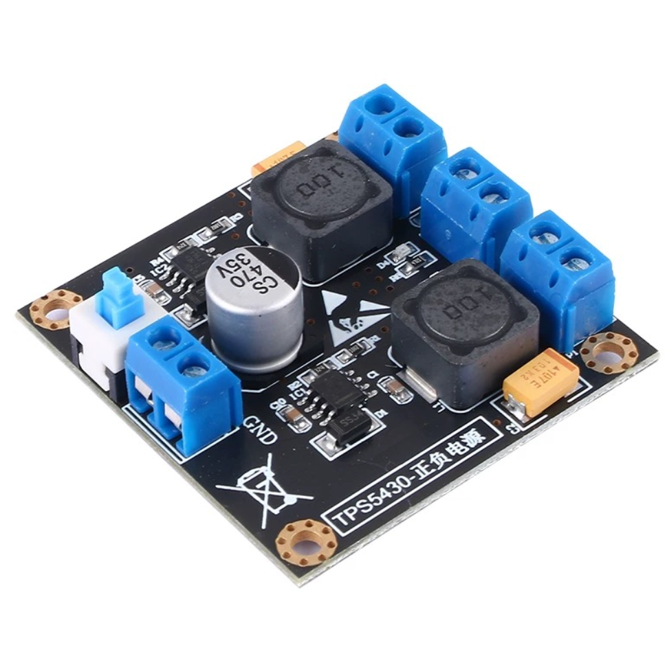
Module Overview
The module supports high current output up to 3A (4A peak) with a wide input voltage range of 5.5V to 28V. In ideal conditions, the conversion efficiency can reach up to 95%, although real-world efficiency is typically around 88%, especially when generating negative voltage outputs. It operates at a fixed 500kHz switching frequency, ensuring relatively low output ripple and good transient response. The module includes overcurrent protection and thermal shutdown, improving safety during operation. A built-in enable function allows low standby power consumption, with shutdown current as low as approximately 17µA.
Positive and Negative Output Design
A key feature of this module is its ability to generate dual power rails (positive and negative outputs), such as ±5V, ±12V, and ±15V depending on configuration. The positive rail generally maintains higher efficiency, while the negative voltage conversion efficiency is slightly lower because additional conversion stages. Typical output equations are Vout+ = 1.221 × (R1/R2 + 1) and Vout− = −1.221 × (R3/R4 − 1), making it suitable for analog circuits requiring symmetrical power supplies.
Key Electrical Parameters
Parameter | Value (with Notes) |
Module Type | Switching Power Supply (DC-DC Buck Converter) |
Input Voltage | 5.5V – 28V (Recommended below 28V; for ±15V output keep input < 21V) |
Output Voltage | Adjustable (Typical ±5V, ±12V, ±15V configurations available) |
Output Current | 3A max (Positive rail), ~2.5A max (Negative rail; not for long continuous full load) |
Input–Output Dropout | ~1V (Minimum required voltage difference for proper regulation) |
Output Power | ~15W (Example: 5V/3A condition, reference only) |
Static Current | ~16mA (No-load quiescent current) |
Switching Frequency | 500kHz (Fixed frequency operation) |
Efficiency | Up to 95% (Theoretical), ~88% real-world (lower for negative rail) |
Output Ripple | ~24mV (Positive output), ~50mV (Negative output, varies with load) |
Module Protection | None (No reverse polarity protection or external fuse included) |
Module Features | Low noise, low ripple design, power indicator LED included |
Module Weight | ~25g |
Module Size | 50 × 50 × 12 mm (L × W × H) |
Operating Temperature | 0°C – 70°C (Consumer-grade operating range) |
Interface | 5.08-2P × 4 terminal blocks |
Module Features
The module is designed with low noise and low ripple performance, making it suitable for sensitive analog circuits. It includes a power indicator LED and follows standard PCB layout practices to reduce electromagnetic interference. However, it does not include reverse polarity protection or external fuse protection, so require careful input handling.
Module Applications
This dual-output module commonly use in operational amplifier power supplies, ADC/DAC reference circuits, industrial automation systems, communication equipment, LED lighting systems, test and measurement instruments, and student electronics competitions as well as DIY projects.
The TPS5430 dual switching power supply module offers a compact, efficient, and flexible solution for generating both positive and negative voltage rails from a single DC input. Its combination of high efficiency, low ripple, and dual-output capability makes it especially useful in analog and mixed-signal circuit designs where require stable symmetric power.
TPS5430 Datasheet
To fully understand the design and performance, refer to the official datasheet provided by Texas Instruments.
Frequently Asked Questions [FAQ]
What is the package type of the TPS5430DDAR?
The TPS5430DDAR from Texas Instruments comes in an 8-pin SOIC PowerPAD™ package. This package includes an exposed thermal pad that improves heat dissipation. Designed for high-current switching regulator applications, allowing efficient thermal performance while maintaining a compact PCB footprint suitable for industrial and power electronics designs.
What is the TPS5430 used for?
Use the TPS 5430 as a step-down (buck) DC-DC converter to efficiently convert higher DC voltages (such as 12V or 24V) into lower regulated voltages. Commonly use in consumer electronics, industrial systems, LED drivers, battery-powered devices, and distributed power systems requiring stable and efficient voltage regulation.
What is price of TPS5430?
The TPS5430 typically costs around 0.5 to 2 USD per piece, depending on supplier, packaging type, and purchase quantity. Bulk orders significantly reduce the unit price. Variants such as TPS5430DDAR and TPS5430DDAG4 may also have slight pricing differences based on distribution channels and availability.
What is the maximum operating voltage for TPS5431 and TPS5430?
The TPS 5430 supports a maximum input voltage of 36V, making it suitable for 24V industrial buses. The TPS5431 supports a lower maximum input voltage of 23V, designed for lower-voltage power rails. Both devices share similar architecture but differ mainly in input voltage capability and application range.
How does the TPS5430 minimize external components?
The TPS5430 minimizes external components by integrating internal loop compensation, a high-side MOSFET, soft-start circuitry, and protection functions into the chip. This reduces the need for external compensation networks and control circuitry, allowing designers to use only essential passive components like an inductor, diode, and feedback resistors.
Conclusion
The TPS5430 from Texas Instruments is a highly efficient and versatile step-down (buck) DC-DC converter designed for a wide range of power management applications. With its wide input voltage range, high output current capability, and integrated MOSFET, it delivers reliable performance while keeping external component count low.
Its built-in features such as internal compensation, soft-start, voltage feedforward, and multiple protection mechanisms make it easy to design stable and robust power supplies without complex circuitry. The availability of compact PowerPAD™ packaging also ensures good thermal performance in space-constrained designs.
Overall, the TPS 5430 is an excellent choice for engineers working on 12V/24V systems, industrial equipment, consumer electronics, LED drivers, and battery-powered applications, offering a strong balance of efficiency, simplicity, and reliability.
Read More:
1. Mini MP1584 DC-DC 3A Buck Converter Module: Complete Guide
2. DRV8833 Dual H-Bridge Motor Driver Module: Complete Guide
3. LM2596S Buck Converter IC & LM2596 S DC-DC Step Down Module
HOT NEWS
Understanding A 0603 Resistor
0603 resistor,dimensions,marking code, values
2025-05-29
The 0402 Resistor: A Comprehensive Guide
0402 Resistor
2025-05-06
LR41 Battery Guide: Specifications, Equivalents, and Uses
LR41 Battery Specifications, Equivalents, and Uses
2025-12-14
MT3608 Boost Converter - An In-Depth Guide
MT3608 Boost Converter
2025-09-04
What Is A 1206 Resistor?
1206 resistor dimensions,footprint,value
2025-06-05
TP4056 Charging Module Pinout, Working, and Applications
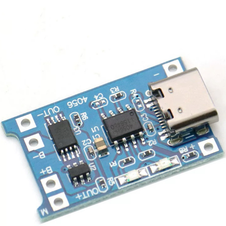
TP4056 Charging Module Pinout, Working, and Applications
2026-01-23
Everything You Need To Know About ARE1309 Relay

2025-04-23
Complete Guide to the 220 Ohm Resistor
220 Ohm Resistor
2025-07-28
120 Ohm Resistor- Specifications, Applications, and Features
2025-05-12
Guide To The AMS1117 Voltage Regulator
AMS1117 Voltage Regulator Circuit
2025-08-17